
In PCB design guidelines chip makers recommend using VLP (very low profile) and HVLP (hyper very low profile) copper to mitigate insertion loss caused by the skin effect – But do you know what happens to the copper surface roughness during PCB fabrication?
Signal integrity is becoming more and more important in High Frequency and High-Speed PCB designs. Signal integrity is impacted by many factors such as insertion loss, return loss and crosstalk. In this blog post we focus on insertion loss and how Aspocomp helps you to mitigate it in PCB manufacturing.
Copper Surface Roughness, Skin Effect and Insertion Loss
Usually with direct current (DC) and low frequency alternating current (AC) applications it does not matter much how rough the copper surface profile of a trace is. Now that the modern digital systems designed for 5G, cloud computing, autonomous driving and other advanced applications are requiring increasingly higher frequencies, the copper surface roughness has a greater impact on signal losses. Therefore copper surface roughness plays a key role in signal integrity. The importance of surface roughness is magnified by the skin effect.
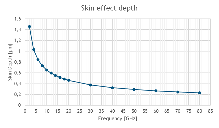
“At frequency of 80GHz the skin depth can be as thin as 0.21µm only”
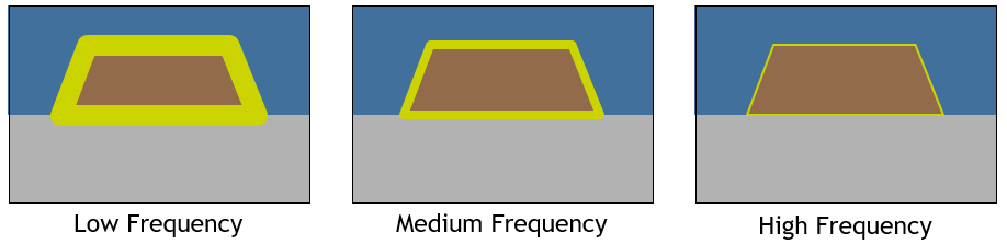
Skin effect means the signal’s tendency to travel through a conductor on its outer surface (skin). At lower frequencies, the current travels through the entire cross-section of the conductor but when the frequency goes up the skin gets thinner. At frequency of 80GHz the skin depth can be as thin as 0.21µm only. This is illustrated in the picture below where the yellow part shows the skin depth on a copper trace.
Chip makers are now recommending the use of low-surface-roughness copper foils such as very low profile (VLP) and hyper very low profile (HVLP) to mitigate insertion loss caused by the skin effect. This is needed because skin effect reduces the cross-sectional area of the channel, increasing the copper resistance. On a rough copper surface the effective signal path length can be much longer than actual trace length.
Why is Signal Integrity more important now than before?
Usual mechanism used in telecommunication is a non-return-to-zero (NRZ) line code. It is a form of digital data transmission in which the binary low and high states, represented by numerals 0 and 1, are transmitted by specific own voltage levels. There must be enough room between these voltage levels to distinguish them.
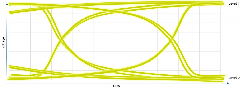
The quality of signal integrity can be easily seen in eye diagram where the altering voltage levels of a signal are forming an eye shaped form. Figure below illustrates the eye diagram of a good quality NRZ signal.
Noise margin is the ratio by which the signal exceeds the minimum acceptable amount. It is normally measured in decibels. In a digital circuit, the noise margin is the amount by which the signal exceeds the threshold for a proper ‘0’ or ‘1’.
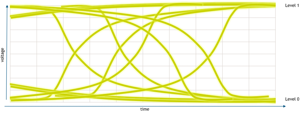
Skew is the time delta between the actual and expected arrival time of a clock signal. Skew can be either extrinsic or intrinsic. Intrinsic can be caused by propagation delays which in part can be caused by skin effect and too rough copper surface. In an eye diagram of a skewed signal the eye is not anymore open and the receiving system cannot interpret the signal.
Picture below illustrates a skewed signal where the eye of the diagram is not anymore open.
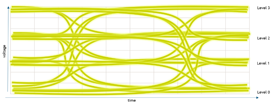
Signal integrity is extremely important now that signal processing is more and more moving to Pulse-Amplitude-Modulation (PAM4) instead of NRZ. PAM4 signaling uses four distinct voltage levels to encode two bits of data per time period. This means doubling the bandwidth by using same frequency. The eye diagram below helps understanding why PAM4 has remarkably reduced noise margin compared to NRZ and therefore the increased importance of signal integrity in PAM4.
What happens to copper surface roughness in PCB shop?
Multilayer PCB manufacturing requires the copper layers and dielectric prepregs to be bonded together. This is done by pressing them together by applying high temperature and pressure. The risk of delamination is traditionally mitigated by roughening the copper surface before pressing the layers together. High copper surface roughness is good for bonding performance but it is not good for signal integrity due to the skin effect. For high frequency and high-speed applications a lower surface roughness is required and it cannot be met with traditional bonding enhancement processes used in PCB fabrication. Reduced etch depth in bonding enhancement can only be reached by using new manufacturing technologies such as MKS (former Atotech) BondFilm EX.
“Lower surface roughness cannot be met with traditional bonding enhancement processes used in PCB fabrication”
Picture below illustrates the difference between rough copper surface and reduced etch depth as well as their effect to the signal path length.

Aspocomp first in Europe
Aspocomp is the first European PCB manufacturer to implement MKS (Former Atotech) BondFilm EX process. This is a new revolutionary bonding enhancement process consisting of brand new equipment and chemistry that ensures excellent adhesion with smooth copper surface.
This investment has been one part of Aspocomp’s 10 million euro investment program in Oulu PCB factory.
Let’s improve your High Frequency PCBs
We have conducted comprehensive signal integrity tests resulting in measurable improvements in signal integrity. Our partner in the study was Polar Instruments UK (https://www.polarinstruments.com/) and the PCB’s measured were manufactured in our Oulu plant.
Contact us if you would like to discuss the results and benefits to your business.
Please contact us
By Antti Ojala