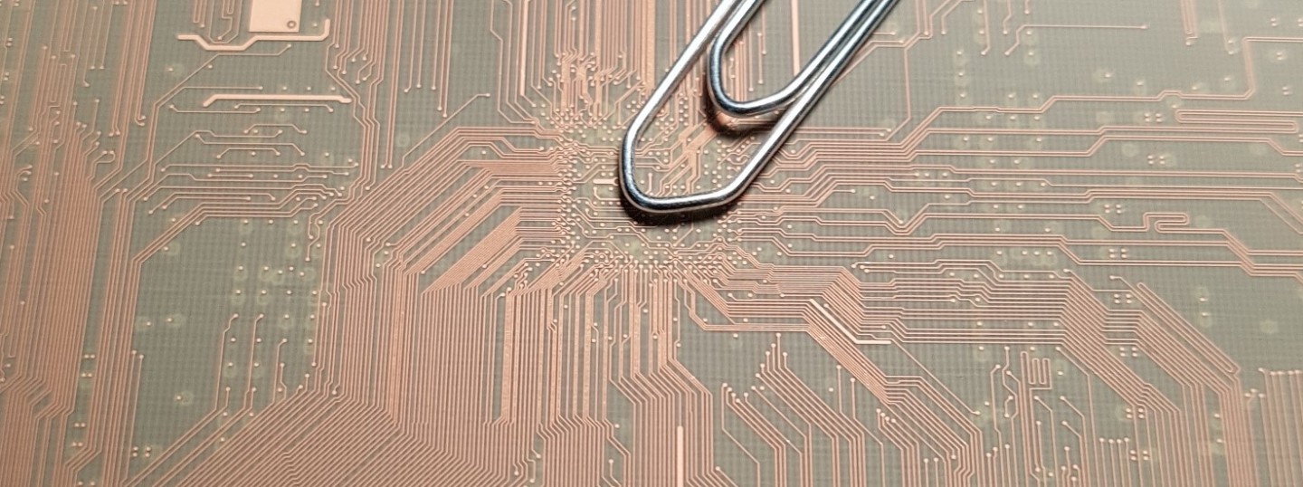
High Density Interconnection (HDI) technology is needed in PCB design to achieve higher wiring density than in conventional PCBs.
HDI PCBs have microvias that are drilled by laser from one layer to the next. Microvias can be staggered or stacked on top of each other. Aspocomp started microvia PCB production in Oulu back in 1998.
Viafilling of microvias is needed to provide connections between stacked microvias or on the top layer to flatten the surface of the microvia. Aspocomp has utilized HDI viafill technology at its Oulu plant since 2008.
Advanced HDI is a technology that goes beyond ordinary HDI processes. Advanced HDI typically features several stacked HDI layers and even anylayer technology where all connections are implemented with microvias.
HDI and Advanced HDI technology enables design for very high density components like 400u pitch BGA with a high amount of I/O pins. This component type usually requires a PCB using multiple layer HDI, for example 4+4B+4 or even anylayer technology. Anylayer technology was introduced at the Aspocomp Oulu plant in 2013.
Aspocomp’s manufacturing is specialized in express production of this PCB type.
See the capability page for more design parameters.


