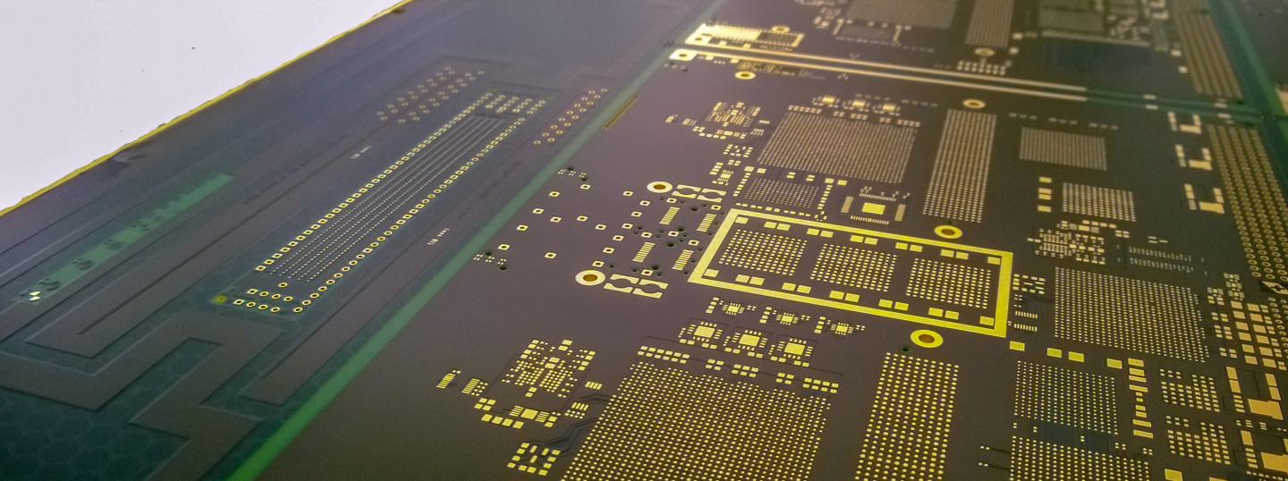
Controlled Impedance Multilayer PCBs for High-Performance Electronics
Aspocomp manufactures high-speed PCBs (digital printed boards) designed for applications where signal integrity, controlled impedance and low transmission loss are critical.
Our high-speed multilayer PCBs are used in telecommunications infrastructure, data center systems, automotive electronics and industrial test equipment where reliable high data-rate performance is required.
Request For Quotation
What is a high-speed PCB?
The term high-speed PCB typically refers to printed circuit boards designed for digital systems operating at high data rates. These are often called high-speed digital PCBs, but the term high-speed PCB is widely used in industry to describe boards designed for controlled impedance and signal integrity.
In high-speed designs, the PCB traces behave as transmission lines. Electrical performance is influenced by:
- Controlled impedance routing
- Dielectric constant (Dk) stability
- Low loss tangent (Df) materials
- Stack-up symmetry and reference plane continuity
- Differential pair routing accuracy
Unlike conventional PCBs, high-speed PCBs require tight manufacturing tolerances to prevent:
- Reflections
- Crosstalk
- Electromagnetic interference (EMI)
- Insertion loss
High-speed PCB design typically becomes critical in multi-gigabit digital systems and high-frequency mixed-signal applications.
Use cases – where high-speed PCBs are required
High-speed digital PCBs are commonly used in:
- 5G base stations and telecom backhaul systems
- Network switches and routers
- Data center servers and high-performance computing (HPC) systems
- Automotive ADAS and in-vehicle networking
- Semiconductor test systems and automated test equipment (ATE)
- Industrial control systems with high-speed interfaces
These systems require controlled impedance multilayer PCBs to ensure reliable signal transmission over complex routing structures.
Key benefits of high-speed PCBs
| Benefit | Description |
| Controlled signal integrity | Precision impedance control reduces reflections and signal distortion. |
| Low transmission loss | Optimized material selection minimizes dielectric loss at high frequencies. |
| Differential pair accuracy | Tight geometry control ensures balanced high-speed signaling. |
| Reliable multilayer construction | Stable stack-up design supports complex routing and high layer counts. |
| Long-term reliability | Built for demanding electrical, thermal and mechanical environments. |
Technical capabilities – High-speed PCB manufacturing
| Feature | Specification |
| Layer Count | Up to 40 layers (higher available on request) |
| PCB Type | Multilayer high-speed digital PCB |
| Materials | FR-4 variants, High-Tg FR-4, low-loss laminates (e.g. high-speed grade materials) |
| Impedance Control | Tight tolerance impedance control per customer specification |
| Min. Track/Space | 50/50 µm (2/2 mil) |
| Via Technology | Through-hole, blind, buried, laser-drilled microvias |
| Impedance Verification | TDR measurement using impedance test coupons |
| Standards | IPC-A-600 Class 2, Class 3, Class 3DS |
| Testing | AOI, X-ray inspection, Flying Probe, electrical test |
Aspocomp supports early stack-up definition and controlled impedance PCB planning during the design phase.
Manufacturing process – how we produce high-speed PCBs
1. Design for manufacturability (DFM) review
We evaluate stack-up, transmission line geometry, impedance targets and material selection.
2. Controlled impedance fabrication
Precision etching and lamination processes maintain dielectric thickness and trace geometry.
3. Impedance and structural verification
TDR measurement verifies controlled impedance performance. AOI and X-ray confirm structural integrity.
4. Electrical testing and final inspection
All boards undergo electrical verification and IPC-compliant inspection prior to delivery.
Risks in high-Speed PCB manufacturing – and how we mitigate them
| Common Challenge | Mitigation |
| Impedance mismatch | Tight process control and impedance verification |
| Dielectric variability | Qualified laminate suppliers and incoming inspection |
| Signal degradation | Optimized stack-up and geometry control |
| Layer misalignment | Precision lamination and X-ray inspection |
| Traceability | Raw material to final product traceability |
| Crosstalk | Implementing stitching vias on the design, but be careful – too many vias will cause problems in PCB manufacturing and increase cost |
| Via reliability issues | IPC Class 3 compliant fabrication processes |
| Stub elimination | Back drilling technology removes unused via stubs to maintain signal integrity in high-speed multilayer PCBs |
Is a high-speed PCB the right choice?
High-Speed Digital PCB is ideal when:
- Your design uses multi-gigabit interfaces
- Signal integrity is a critical system requirement
- Differential pair routing is required
- EMI control is important
- You require a controlled impedance PCB manufacturer
A standard PCB may be sufficient when:
- Signal speeds are moderate
- Impedance control is not critical
- Cost sensitivity outweighs performance requirements
High-speed PCB vs standard PCB
| Feature | High-Speed PCB | Standard PCB |
| Impedance control | Required and verified | Often not specified |
| Signal integrity | Optimized | Basic |
| Materials | Low-loss laminates available | Standard FR-4 |
| Layer complexity | Multilayer routing optimized | Simpler stack-ups |
| Applications | Telecom, data center, automotive | General electronics |
Frequently Asked Questions
What is controlled impedance in a PCB?
Controlled impedance means that specific PCB traces are manufactured to a defined characteristic impedance value, determined by trace geometry and the dielectric properties of the surrounding laminate. When matched to the source and load impedances, this ensures maximum signal transfer and minimizes reflections in high-speed designs.
At what speed is a high-speed PCB required?
High-speed design considerations typically apply in multi-gigabit digital systems or where fast edge rates make transmission line effects significant.
Do you manufacture multilayer high-speed PCBs?
Yes. Aspocomp manufactures multilayer controlled impedance PCBs for demanding high-speed applications.
Which materials are best for high-speed PCBs?
Low-loss laminates with stable dielectric properties are typically used (e.g. Panasonic Megtron series, Isola MT40, Tachyon100G and others). Material selection depends on frequency, layer count and system requirements.
Engineering Authority
Content reviewed by the Aspocomp Engineering Team — specialists in high-speed digital PCB manufacturing, controlled impedance production, and IPC Class 3 compliance.
Aspocomp is a Finnish PCB manufacturer with its own production facility in Oulu, Finland, and a qualified partner network across Europe and China. Our engineering team has accumulated deep specialist knowledge in demanding high-technology PCB manufacturing, and we work closely with our customers from the earliest design stages to ensure the best possible outcome for every project.
Talk to Our High-Speed PCB Experts
Ready to discuss your next high-speed digital PCB project? Our engineering team is available to review your design, advise on material selection and stack-up, and provide a detailed manufacturing quote.