News from the factory floor
Roughly 35% of the PCB designs that we manufacture in Oulu on monthly basis are in production for the first time. That is our learning process and it gives input to the investment program and production methods development.
Here is a snapshot of what we have been developing for the past year.
Outer Layer Lamination
A new autocut sheet laminator, Hakuto 630NP has been taken into use. This new machine processes all of the PCB that we manufacture and it is a powerful piece considering the small size of 1,5 m * 2,5 m.
The improvement over the older machine is better programmability for different board types and resist needs.
Horizontal final curing
A new UV-IR oven is fully automated and replacing the old UV curing machine which was manually loaded. It does include UV part where solder mask is exposed to UV light which will cure solder mask and after that in line is IR oven where panels are heated with infra-red. In the oven the rest of the solvents will evaporate and solder mask will be final cured.
After UV curing there will be loader-unloader which can be used to unload panels after UV curing, or it can let panels go through to IR-oven, or it can load panels to IR oven without being UV cured. This investment does replace old conventional baking ovens so these can be used to other purposes and that way release capacity to other parts of the factory.
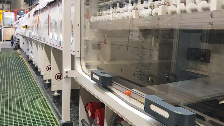
SES line with automation
The installation of the 26 m long Schmid SES line will be finished around mid-February and this replacement investment is also part of the longer-term upgrade investments of the factory. We expect quality improvements in addition to 100% increase in the etching capacity. Now we can better process boards that contain a lot of copper. New loaders will increase speed and release human resources for other parts of manufacturing process.
Plugging machine upgrade
Our 1,5 years old ITC plugging machine will now get a second plugging unit. This upgrade will increase quality and thus give us overall better yield in the production process. And the straightforward capacity will increase by 100% as well. Savings in the epoxy are expected too.
More than 50% of the boards are plugged and as they contain maybe tens of thousands of holes to be plugged, quality improvement will lead to overall yield improvement. Missing plugging even a single hole will lead to discarding the PCB.
On the process side
We have put effort into combining coin + inlay in the same board and perfecting the process of wireless hard gold.
Coin and inlay design can be needed in applications that have digital and RF-functionalities in the same board. There are many details to match in materials compatibility, mechanical strength, stretching factors and stacking up the different layers.
A PCB factory is an ever evolving combination of a lot of machinery and processes – here we have written about some of the things that have been renewed. As said some 35% of the boards every month are new designs in our own factory, and thus teach us something new every day.
You are welcome to contact our sales team with any questions.