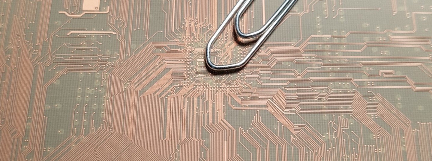
High-density interconnect PCB Manufacturing for Ultra-compact electronics
Aspocomp manufactures HDI PCBs and advanced HDI multilayer boards designed for applications where extreme wiring density, miniaturization and electrical performance are critical.
Our HDI PCB manufacturing facility in Oulu, Finland has been developing microvia technology since 1998, delivering reliable advanced HDI, stacked microvia and anylayer PCB solutions for various industries.
Talk to an Engineer
What is an HDI PCB?
A High-Density Interconnect (HDI) PCB is a printed circuit board technology that enables significantly higher wiring and component density than conventional multilayer PCBs.
HDI boards achieve this using:
- Laser-drilled microvias
- Sequential lamination
- Fine line routing
- Via-in-pad structures
These technologies allow electrical connections between layers with extremely small vias, enabling more complex routing in a smaller footprint.
Advanced HDI and anylayer PCBs
Advanced HDI structures extend this concept by using stacked microvias and multiple HDI buildup layers, allowing extremely dense interconnect structures.
Anylayer PCB technology (also known as ELIC – Every Layer Interconnect) allows microvias to connect any layer to another layer within the board. This architecture provides maximum routing flexibility and is essential for designs using ultra-fine pitch components such as 0.4 mm BGA packages.
The result is a PCB platform that enables extreme miniaturization without compromising electrical performance or reliability.
Typical use cases for advanced HDI PCBs
HDI PCBs are widely used in electronics where compact design and high routing density are essential.
Typical applications include:
Semiconductor test equipment
ATE load boards and probe cards for testing high-pin-count ICs.
Mobile and consumer electronics
Smartphones, tablets and wearable devices requiring extremely compact PCB layouts.
Automotive electronics
Advanced sensor modules, ECU systems and automotive communication electronics.
Medical devices
Miniaturized diagnostic equipment and implantable electronics.
Aerospace and defense systems
Compact avionics and communication modules where size and reliability are critical.
Key benefits of advanced HDI PCBs
| Benefit | Description |
| Extreme miniaturization | Stacked microvias and anylayer interconnects allow extremely compact product designs. |
| Higher routing density | Microvias and via-in-pad enable complex routing for high-pin-count components. |
| Superior electrical performance | Shorter signal paths reduce parasitic capacitance, crosstalk and signal loss. |
| Design flexibility | Anylayer connectivity allows designers to route signals freely between layers. |
| Proven reliability | Mature copper via-filling processes ensure robust interconnections under thermal stress. |
Technical capabilities – Advanced HDI PCB manufacturing
| Feature | Specification |
| PCB technology | HDI, Advanced HDI, Anylayer (ELIC) |
| Layer count | Up to 40 layers (project dependent) |
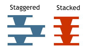
| Microvia structures | Stacked microvias, staggered microvias |
| Via technology | Copper-filled microvias, Via-in-Pad (VIP) |
| Min. via size | 0.1 mm laser-drilled |
| Min. track / space | 50/50 µm (2/2 mil) |
| BGA pitch support | Down to 0.4 mm |
| Standards | IPC-2226 HDI design standard, IPC Class 2 / Class 3 |
| Inspection & testing | AOI, X-ray inspection, Flying Probe, cross-section analysis |
Aspocomp provides engineering support for HDI stack-up planning, microvia structures and manufacturability analysis during the design phase.
Our HDI manufacturing process
Aspocomp’s HDI PCB manufacturing process combines advanced microvia fabrication with strict quality control.
1. Engineering and DFM review
Our engineers analyze the stack-up structure, dielectric materials and via architecture to ensure manufacturability and reliability.
2. Laser drilling and microvia formation
High-precision laser drilling systems create microvias, followed by a controlled copper plating process that ensures reliable via filling.
3. Sequential lamination and buildup
Multiple HDI layers are built through sequential lamination, allowing stacked microvia structures and extremely dense routing.
4. Inspection and reliability verification
Each production stage includes AOI and X-ray inspection, while cross-section analysis verifies the integrity of microvia structures.
Common risks in HDI PCB manufacturing and how Aspocomp mitigates them
| Challenge | Aspocomp Mitigation |
| Microvia reliability issues | Controlled copper via-fill process ensures robust stacked microvia structures. |
| Layer misalignment | Advanced registration systems and X-ray inspection during lamination. |
| Material delamination | Carefully selected dielectric materials and tightly controlled lamination cycles. |
| Yield on complex HDI designs | Extensive DFM analysis and in-process quality control. |
Is an advanced HDI PCB right for your project?
Advanced HDI PCBs are ideal when:
- Your design includes fine-pitch BGAs (<0.5 mm)
- Maximum component density and miniaturization are required
- Complex routing is needed for high I/O counts
- Signal integrity and electrical performance are critical
Standard PCBs or basic HDI boards may be sufficient when:
- Component pitch is larger than 0.8 mm
- High routing density is not required
- Cost is the primary design constraint
Advanced HDI PCB vs Standard PCB
| Feature | Advanced HDI / Anylayer PCB | Standard PCB |
| Via technology | Laser-drilled microvias | Through-hole vias |
| Routing density | Extremely high | Moderate |
| Component pitch | <0.4 mm | >0.8 mm |
| Board size | Smaller and lighter | Larger |
| Manufacturing complexity | High | Moderate |
| Typical applications | Smartphones, test equipment, medical devices | Industrial electronics |
Frequently asked questions
What is an HDI PCB?
An HDI PCB is a printed circuit board technology that uses laser-drilled microvias and fine line routing to achieve high wiring density and miniaturized electronic designs.
What is the difference between stacked and staggered microvias?
Stacked microvias are placed directly on top of each other across multiple layers, enabling maximum routing density. Staggered microvias are offset between layers and may offer improved manufacturability.
What is Anylayer or ELIC technology?
Anylayer (Every Layer Interconnect) PCB technology allows microvias to connect any layer within the PCB stack-up, providing maximum routing flexibility for ultra-dense designs.
Why is via filling important in HDI boards?
Copper via filling is required for stacked microvias and Via-in-Pad structures. It creates a flat surface for component mounting and ensures strong electrical and thermal connections.
Engineering expertise
Content reviewed by the Aspocomp Engineering Team – specialists in HDI PCB manufacturing since 1998.
Aspocomp’s Oulu facility was among the first in Europe to industrialize microvia technology. Our long experience with stacked microvias, via-fill processes and anylayer interconnect technology enables reliable manufacturing of complex HDI designs for demanding industries.
Talk to our HDI PCB experts
Ready to develop your next HDI design?
Our engineers can assist with:
- stack-up planning
- microvia architecture
- DFM analysis
- material selection